Starting point: Chapters 1–10; physical concepts and approximations are introduced as needed.
Anchor example: Two electron spins with a tunable exchange interaction.
This lesson includes explanations, worked examples, and problems with solutions. Advanced results whose proofs are outside the chapter are identified explicitly.
Ions and neutral atoms are held by fields in a vacuum chamber. A semiconductor chip, made with the methods of ordinary electronics, could hold far more qubits in a small area, if one trapped electron could serve as a qubit. An electron's charge is easy to move and to sense, but charge also couples to every stray field. Can an electrical device store information in an electron's spin, and move charge only when it needs to operate on that information?
We first ask what two-state property an electron carries, and how a magnetic field turns it into a qubit with a definite frequency. Confining the electron in a small region and choosing one or two spins as the encoding then gives a way to prepare it. Moving the electron through a magnetic gradient gives spin rotations from electrical signals. Letting two electrons tunnel toward each other gives exchange, and exchange gives SWAP. Finally, reading a spin requires converting it into charge first, and disorder in the material limits how uniform many such devices can be.
Our first question is what two-state property an electron carries even when its position is fixed.
11.1 Spin Qubits
An electron trapped in a semiconductor has charge, motion, and spin. Which of these should hold the qubit, and how is it prepared? The spin, split by a magnetic field, gives two levels that charge noise touches only weakly. Choosing one spin or a pair of spins as the encoding, and letting electrons tunnel selectively to a reservoir, then gives preparation.
11.1.1 Confinement and Zeeman splitting
What two-state property does an electron carry even when its position is fixed? We take it as a physical input. Every electron has an intrinsic angular momentum called its spin. Measured along any chosen axis, the spin gives one of only two values, called up and down. So the spin states of one electron form a qubit.
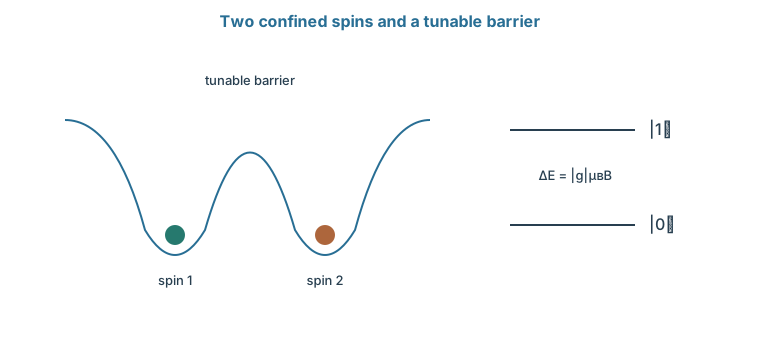
How do we give the two states different energies? With the spin comes a magnetic moment \(\vec\mu\), and a second physical input says that a moment in a magnetic field \(\mathbf B\) has energy \(-\vec\mu\cdot\mathbf B\). For an electron the resulting splitting is \(\Delta E=|g|\mu_BB\). Here \(\mu_B\) is a fundamental constant called the Bohr magneton, and the g-factor \(g\) is about 2 for a free electron and depends on the material inside a solid. This splitting is the Zeeman splitting.
Label the lower spin state zero, so the qubit Hamiltonian is \(-\Delta EZ/2\). For \(|g|=2\), \(B=0.5\) T, and \(\mu_B/h\simeq14\) GHz/T, the qubit frequency is 14 GHz. The sign of \(g\) decides which physical spin orientation is the lower state.
Where is the electron held? Voltages on electrodes above the semiconductor form a small potential well that holds a single electron. This well is called a quantum dot. The electron's motion in the dot has its own energy levels, called orbital levels. In silicon there is a further pair of nearly equal low-lying states, called valley states, which come from the crystal's structure. Orbital and valley states lie outside the chosen spin pair, and they must be far enough above it for the applied controls and the temperature.
11.1.2 Spin encodings
Must one spin be one qubit? One electron spin supplies two basis states. A pair of spins can instead encode a qubit in \(\ket S=(\ket{01}-\ket{10})/\sqrt2\), the singlet, and \(\ket{T_0}=(\ket{01}+\ket{10})/\sqrt2\), one of the three triplets. These two states have the same total spin along the field, so a uniform field shifts them equally. They respond differently to the interaction between the spins and to a difference in field between the two dots. A different encoding thus changes which noise is suppressed and which controls are available. Using extra spins is not by itself error correction.
How do we prepare a single spin? A nearby reservoir of electrons is filled up to a certain energy, its chemical potential. Set that energy between the two spin levels of the dot. An electron in the upper spin state can then tunnel out to the reservoir, and an electron can tunnel back in only into the lower state. After a short wait the dot holds a lower-spin electron. This requires the reservoir temperature and the widths of the levels to be small compared with the splitting, and the loading time to be controlled. Thermal relaxation is another route to the same state.
The orbital confinement and spin splitting are different energy scales. Exchange depends on wavefunction overlap across the barrier; physical dot positions alone do not specify the gate.
Problem 11.1. For \(|g|=2\), \(B=0.5\) T, and \(\mu_B/h\approx14\) GHz/T, find the spin frequency.
Worked solution
The frequency is 2 × 14 × 0.5 = 14 GHz. This is an illustrative effective-g model, not a universal value for semiconductor devices.
11.2 Electrical Control
A spin responds to magnetic fields, but a chip is driven by voltages. How can an electrical signal rotate one spin, and how can two spins interact? Moving the electron through a field that varies in space turns a voltage into an oscillating magnetic field. Letting two electrons tunnel toward each other gives an exchange interaction whose strength the voltages control.
11.2.1 Spin rotations
How can a voltage rotate a spin? An oscillating magnetic field across the spin gives an off-diagonal drive term, and at resonance the familiar Rabi oscillations follow. Such fields are hard to confine to one dot, though. Suppose instead that the static field varies in space, with gradient \(\partial B/\partial x\). An oscillating voltage that moves the electron by \(\delta x\) then changes the field it feels by \((\partial B/\partial x)\delta x\). So the electron sees an oscillating magnetic field produced by an electrical signal.
How fast does it rotate? The Rabi frequency scales as \(|g|\mu_B(\partial B/\partial x)\delta x/\hbar\), with a numerical factor that depends on how the oscillating component is defined. In many materials a second route exists, spin–orbit coupling, which links the electron's motion directly to its spin. Both mechanisms let gate electrodes control the spin. Both also let fluctuating charges near the dot perturb it.
11.2.2 Exchange gates
How do two spins in neighbouring dots interact? Through their charge. Let an electron tunnel between the dots with tunnelling energy \(t_c\), and let putting both electrons in one dot cost the large energy \(U\). We also need a physical input, the Pauli exclusion principle: two electrons in the same orbital must be in the singlet spin state. So a triplet pair cannot tunnel into one dot, while a singlet can.
What does this do to the singlet's energy? The singlet with one electron per dot couples, with strength \(\sqrt2t_c\), to each of the two states with both electrons in one dot. A state coupled weakly by \(c\) to a state an energy \(U\) above it is pushed down by about \(c^2/U\), the same expansion that gave the light shift. With two such couplings the singlet moves down by \(4t_c^2/U\), while the triplets do not move. The two electrons never actually sit together; the energy shift comes from this virtual tunnelling. The singlet–triplet splitting is the exchange energy
\[J\simeq\frac{4t_c^2}{U},\]
valid when \(t_c\ll U\) and other levels are far away.
Which Hamiltonian has this splitting? Write \(H=J\mathbf S_1\cdot\mathbf S_2\) with \(\mathbf S=(X,Y,Z)/2\), so \(J\) is an energy. Checking each basis state shows that \(XX+YY+ZZ=2\,\mathrm{SWAP}-I\). SWAP is \(+1\) on the triplets, which are symmetric, and \(-1\) on the singlet. So the singlet has energy \(-3J/4\) and every triplet \(+J/4\). After a time \(t\) their relative phase is \(e^{iJt/\hbar}\).
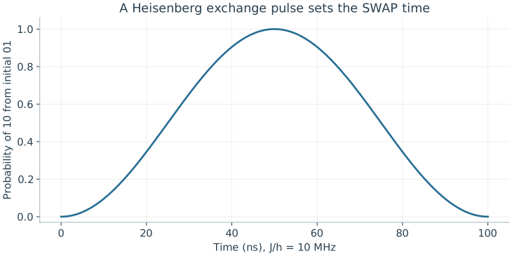
What gate does this give? Since \(\ket{01}=(\ket{T_0}+\ket S)/\sqrt2\), the probability of finding \(10\) is \(\sin^2[Jt/(2\hbar)]\). At \(Jt/\hbar=\pi\) the singlet's sign reverses relative to the triplets, which implements SWAP up to a global phase. Half that pulse gives an entangling square root of SWAP. With \(J/h=10\) MHz these take 50 ns and 25 ns. Note that \(J\) here is an energy, whereas the \(J\) of the ZZ coupling was an angular frequency.
The stated exchange-energy convention gives SWAP at 50 ns and an equal-weight entangling state at 25 ns. This differs from the angular-frequency g convention used for exchange between circuits.
Problem 11.2. If \(J/h=10\) MHz, how long is a SWAP exchange pulse?
Worked solution
\(Jt/\hbar=2\pi(10^7)t=\pi\), so \(t=50\) ns; the square-root pulse takes 25 ns in the ideal constant-exchange model.
11.3 Readout and Integration
A spin's magnetic moment is far too small to detect directly, but a single electron's charge is easy to sense. How do we turn a spin into a charge signal, and what limits a chip full of such devices? Making the electron's motion depend on its spin converts the qubit into a charge configuration, with errors in both stages. The sensitivity of exchange to voltages and disorder then sets how uniform many devices can be.
11.3.1 Spin-to-charge conversion
How can a charge sensor read a spin? A conversion step must first make the charge configuration depend on the spin. One method reuses selective tunnelling: with the reservoir energy between the spin levels, an upper-spin electron leaves the dot and a lower-spin electron stays. Another uses two electrons and the exclusion principle. Tilt the double dot so that both electrons would prefer one dot. A singlet can move there, but a triplet is blocked, so the charge stays split. This is called Pauli blockade.
How do the two stages combine? Let \(c\) be the probability that the conversion produces the correct charge label, and \(d\) the probability that the detector reads that label correctly, with symmetric independent errors. The spin is assigned correctly when both stages succeed, or when both fail:
\[P_{\rm correct}=cd+(1-c)(1-d).\]
Perfect charge detection, \(d=1\), still leaves the success probability \(c\). Temperature, tunnel rates, and the integration window all act before the final electronic discrimination.
11.3.2 Disorder, wiring, and uniformity
Can thousands of dots be made identical? The exchange formula shows why this is hard. Since \(J\simeq4t_c^2/U\), a small fractional change in tunnelling gives \(\delta J/J\simeq2\,\delta t_c/t_c\). The barrier voltage that makes exchange controllable therefore also makes it sensitive to voltage noise and to small differences between devices.
Other sources of variation need their own remedies. Nuclear spins in the host material, charge fluctuations, disorder, and valley splittings call for different controls and materials choices. Dense placement does not guarantee uniform operation, since gates, reservoirs, sensors, and wiring all take space. A dense array becomes a processor only once its exchange and rotations stay calibrated with neighbouring devices active.
Problem 11.3. Can perfect charge detection guarantee perfect spin readout?
Worked solution
No. The spin-to-charge conversion may have failed before detection. The measured assignment error combines both stages and preparation errors unless independently calibrated.
A crystal defect can also hold an electron spin, and it can emit light. Can such a defect join a stationary qubit to a photon that travels?
Worked model check. Let J/h=5 MHz in the stated Heisenberg model. Find the times for SWAP and its entangling square root.
Worked solution
\(Jt/\hbar=\pi\) gives 100 ns for SWAP; half that area gives 50 ns. These values assume constant exchange and negligible competing terms.
Electrostatic quantum dots in isotopically purified silicon or germanium confine single electrons or holes whose spin states serve as sub-micron solid-state qubits.
Exchange interactions \(J(t)\) controlled by barrier gate voltages implement fast \(\sqrt{\mathrm{SWAP}}\) and controlled-phase gates between neighboring dots, while micromagnets or spin–orbit coupling enable electric-dipole spin resonance (EDSR).
Pauli spin blockade and RF single-electron transistors convert spin correlations into measurable charge configurations Compatible with CMOS fabrication.
Questions and worked problems
These exercises draw on the whole chapter. Attempt each question before opening a hint, explain your reasoning, then compare it with the worked solution.
An electron spin with \(|g|=2\) sits in \(B=0.2\) T, with \(\mu_B/h\approx14\) GHz/T. Find the qubit frequency and its thermal excited population at an electron temperature of \(100\) mK, using \(hf/k_B\approx0.048\) K per GHz.
Hint 1
\(f=|g|(\mu_B/h)B\).
Hint 2
\(p_1=1/(1+e^{hf/k_BT})\).
Worked solution
\(f=2\times14\times0.2=5.6\) GHz. Then \(hf/k_B\approx0.27\) K, so at \(100\) mK the ratio is \(2.7\) and \(p_1\approx1/(1+e^{2.7})\approx0.064\). Thermal preparation at this field and temperature leaves over \(6\%\) excited, so spin-selective tunneling or a higher field is needed for good initialization.
With \(H=J\mathbf S_1\cdot\mathbf S_2\) and \(J/h=2\) MHz, find the SWAP time and the \(\sqrt{\mathrm{SWAP}}\) time. What state does \(\sqrt{\mathrm{SWAP}}\) make from \(\ket{01}\)?
Hint 1
SWAP at \(Jt/\hbar=\pi\): \(t=1/(2J/h)\).
Hint 2
\(\ket{01}=(\ket{T_0}+\ket S)/\sqrt2\).
Worked solution
SWAP: \(t=1/(2\times2\ \text{MHz})=250\) ns; \(\sqrt{\mathrm{SWAP}}\): \(125\) ns. At \(Jt/\hbar=\pi/2\), the singlet has gained relative phase \(e^{i\pi/2}=i\), so \(\ket{01}\to\frac{1}{\sqrt2}(\ket{T_0}+i\ket S)=\frac{1+i}{2}\ket{01}+\frac{1-i}{2}\ket{10}\), an equal-weight entangled state.
Spin-to-charge conversion succeeds with \(c=0.98\) and the charge detector reads correctly with \(d=0.99\). Find the spin assignment fidelity \(cd+(1-c)(1-d)\). Which stage limits it?
Hint 1
\(0.98\times0.99+0.02\times0.01\).
Hint 2
Compare the error of each stage.
Worked solution
\(P_{\rm correct}=0.9702+0.0002\approx0.970\). The conversion error (\(2\%\)) dominates the detector error (\(1\%\)); improving the charge sensor alone to perfect would raise fidelity only to \(0.98\). Readout must be optimized at the stage that sets the error.
Exchange depends on a tunnel coupling as \(J\simeq4t_c^2/U\). (a) A \(1\%\) error in \(t_c\) gives what fractional error in \(J\)? (b) For an intended \(\sqrt{\mathrm{SWAP}}\) (\(Jt/\hbar=\pi/2\)), estimate the resulting phase error and gate infidelity \((\delta\phi/2)^2\). (c) Why does this make barrier-gate voltage noise important?
Hint 1
\(\delta J/J=2\delta t_c/t_c\).
Hint 2
Phase error \(=(\pi/2)(\delta J/J)\).
Worked solution
(a) \(\delta J/J\approx2\times1\%=2\%\). (b) The exchange phase is off by \((\pi/2)\times0.02\approx0.031\) rad, giving infidelity of order \((0.031/2)^2\approx2.5\times10^{-4}\). (c) \(t_c\) is set by a gate voltage through an exponential tunnel barrier, so small voltage fluctuations produce larger fractional changes in \(t_c\), and twice that in \(J\). Charge noise on the barrier therefore shows up directly as two-qubit gate error.
Two dots have Zeeman energies differing by \(\Delta E_z/h=50\) MHz (for example from a magnetic gradient), and exchange is off. (a) Show that \(\ket{01}\) and \(\ket{10}\) are split by \(\Delta E_z\). (b) Starting from the singlet \(\ket S\), how long until it has fully converted to \(\ket{T_0}\)? (c) How does this give a second control axis for a singlet–triplet qubit?
Hint 1
\(\ket S\) and \(\ket{T_0}\) are equal superpositions of \(\ket{01}\) and \(\ket{10}\) with opposite relative signs.
Hint 2
Full conversion when the relative phase of \(\ket{01}\) and \(\ket{10}\) reaches \(\pi\).
Worked solution
(a) Each spin contributes \(\mp E_i/2\), so \(\ket{01}\) and \(\ket{10}\) differ in energy by \(E_1-E_2=\Delta E_z\). (b) The relative phase between \(\ket{01}\) and \(\ket{10}\) grows as \(\Delta E_zt/\hbar\); when it reaches \(\pi\), \(\frac{1}{\sqrt2}(\ket{01}-\ket{10})\) has become \(\frac{1}{\sqrt2}(\ket{01}+\ket{10})\) up to a phase. That takes \(t=h/(2\Delta E_z)=10\) ns. (c) Exchange splits \(\ket S\) from \(\ket{T_0}\) (a \(Z\)-like axis in that basis), while the field difference mixes them (an \(X\)-like axis), so pulsing \(J\) and using the gradient gives full control of the two-spin qubit.
In energy-selective readout, an excited spin tunnels out with mean time \(\tau_{\rm out}=10\) μs, the readout window is \(50\) μs, and the excited spin relaxes with \(T_1=1\) ms. (a) Estimate the probability that an excited spin tunnels within the window. (b) Estimate the probability that it relaxes before tunneling. (c) Combine them into the conversion success \(c\) for an excited spin.
Hint 1
\(P(\text{tunnel within }T)=1-e^{-T/\tau_{\rm out}}\).
Hint 2
Relaxing first has probability about \(\tau_{\rm out}/(\tau_{\rm out}+T_1)\).
Worked solution
(a) \(1-e^{-5}\approx0.993\). (b) The two processes compete; relaxation wins with probability about \(\tau_{\rm out}/(\tau_{\rm out}+T_1)\approx0.010\). (c) \(c\approx0.993\times0.990\approx0.98\) for an excited spin. A longer window helps (a) but raises the chance of thermally activated tunneling of the ground spin; faster tunneling helps both (a) and (b) but must stay slow enough for the charge sensor to resolve the event.
An electron is driven electrically back and forth by \(\delta x\) in a magnetic gradient \(\partial B/\partial x=1\) mT/nm, with \(|g|=2\) and \(\mu_B/h\approx14\) GHz/T. (a) For \(\delta x=1\) pm, estimate the oscillating field and the frequency scale \(|g|(\mu_B/h)\delta B\). (b) Repeat for \(\delta x=10\) pm. (c) Why does a large gradient also make the qubit more sensitive to charge noise?
(a) \(\delta B=1\ \mu\)T, giving a frequency scale \(2\times14\ \text{GHz/T}\times10^{-6}\ \text{T}=28\) kHz (the Rabi frequency is of this order, up to a convention factor), so a \(\pi\) pulse takes tens of microseconds. (b) \(10\) pm gives \(280\) kHz and pulses of a few microseconds. (c) Any electric fluctuation that moves the electron also moves it through the gradient and shifts its spin frequency, so the same coupling that enables fast electrical control converts charge noise into dephasing. Device design balances drive speed against this sensitivity.
A student takes the exchange rate \(g/2\pi=10\) MHz from a paper using \(H=\hbar g(XX+YY)/2\) and plugs it into the formula “SWAP at \(Jt/\hbar=\pi\)” with \(J/h=10\) MHz, predicting \(50\) ns. The paper’s SWAP time is \(25\) ns. Explain the discrepancy.
Hint 1
Chapter 4 found full exchange at \(gt=\pi/2\).
Hint 2
The two Hamiltonians normalize the coupling differently.
Worked solution
In the \(XX+YY\) convention with angular frequency \(g\), full swap occurs at \(gt=\pi/2\), so \(g/2\pi=10\) MHz gives \(t=1/(4\times10\ \text{MHz})=25\) ns. In the Heisenberg convention \(J\mathbf S_1\cdot\mathbf S_2\) with \(J\) an energy, SWAP occurs at \(Jt/\hbar=\pi\), giving \(50\) ns for \(J/h=10\) MHz. The two coupling constants differ by normalization (spin-\(\frac12\) operators versus Pauli matrices, energy versus angular frequency, and the presence of a \(ZZ\) term). Numbers cannot be transferred between papers without matching the Hamiltonian they refer to.
Random nuclear spins produce a quasi-static field that varies from run to run, giving a Gaussian spread of qubit frequencies with standard deviation \(\sigma_f\). Using \(T_2^*=\sqrt2/(2\pi\sigma_f)\) for slow Gaussian frequency noise, compare a natural GaAs-like host with \(\sigma_f=10\) MHz and an isotopically purified silicon-like host with \(\sigma_f=10\) kHz. What does echo do in each case, and what does the comparison say about materials choice?
Hint 1
\(\sqrt2/(2\pi\times10^7)\approx22.5\) ns.
Hint 2
An echo refocuses noise that is constant within a run.
Worked solution
The GaAs-like host gives \(T_2^*\approx22.5\) ns; the purified silicon-like host gives about \(22.5\) μs, a thousand times longer. In both cases echo removes the quasi-static part, so echo coherence is limited by how fast the nuclear field changes during a run. Removing nuclear spins altogether, by purifying the host isotope, eliminates the noise source rather than refocusing it, which is why material choice is one of the most powerful levers for spin qubits.
A crossbar addresses an \(N\times N\) array of dots with \(2N\) shared lines, so each dot is controlled by the intersection of a row and a column. (a) Compare the number of lines with one line per dot for \(N=100\). (b) Why does this require uniformity: suppose dot frequencies scatter by \(\pm20\) MHz while a shared pulse has bandwidth \(1\) MHz. (c) What are two ways to cope?
Hint 1
\(2N=200\) versus \(N^2=10^4\).
Hint 2
A shared pulse can only address dots within its bandwidth.
Worked solution
(a) \(200\) lines instead of \(10^4\), a fifty-fold saving that grows with \(N\). (b) Shared lines apply the same pulse to many dots; if their frequencies scatter by tens of megahertz while the pulse is resonant within about a megahertz, a single pulse cannot rotate them all, and different dots need different frequencies, which the shared line cannot supply simultaneously. (c) Improve fabrication uniformity, or use local tuning (individual gate voltages that shift each dot into resonance) and frequency-multiplexed pulses. Wiring savings are only available if variability is controlled.